Semiconductor Test ProbesSemiconductor Testing — High-Temperature Test Probes
C.C.P. developed proprietary high-temperature plating test probes — maintaining contact resistance ≤175mΩ at 200°C for 500 continuous hours — a 20× improvement over standard gold plating. Applications include QFN test modules, IC burn-in testing, ATE automatic test equipment, and WLCSP / BGA test socket probes.
Burn-in testing and IC high-temperature test environments place extreme demands on contact probes — demands that standard gold-plated test probes often cannot meet.
Gold Plating Failure at High Temperature
Standard gold-plated test probes suffer interface diffusion and oxidation within 24 hours at 200°C, causing impedance degradation.
Contact Resistance Degradation
Once impedance exceeds the 175mΩ limit, test failures occur — affecting IC test judgment accuracy and yield.
Frequent Replacement Costs
Short probe lifespan causes frequent downtime for replacement — reducing overall utilization of burn-in test and ATE equipment.
Multi-Package Testing Requirements
QFN, BGA, WLCSP and other package types have widely varying requirements for probe size, pitch, and spring force — demanding custom engineering capability.
C.C.P. Capabilities
C.C.P. Technical Capabilities
C.C.P.’s proprietary high-temperature plating architecture, combined with a stable 30gf spring force structure, has passed complete 200°C / 500H validation.
Proprietary High-Temperature Plating
In-house plating architecture prevents interface diffusion and oxidation at 200°C high temperatures — replacing standard gold plating.
200°C / 500H Validated
Fully passed 200°C continuous 500-hour testing — maintaining contact resistance ≤175mΩ, a 20× improvement over standard gold plating.
96H Salt Spray Pass
Passes 96-hour salt spray testing after high-temperature exposure — no discoloration, no corrosion — ensuring long-term reliability in test environments.
Multi-Package Interface Support
Probe body size and spring force are customizable — supporting QFN, BGA, WLCSP, and various other semiconductor package test requirements.
Application Positions
Semiconductor Test Application Positions
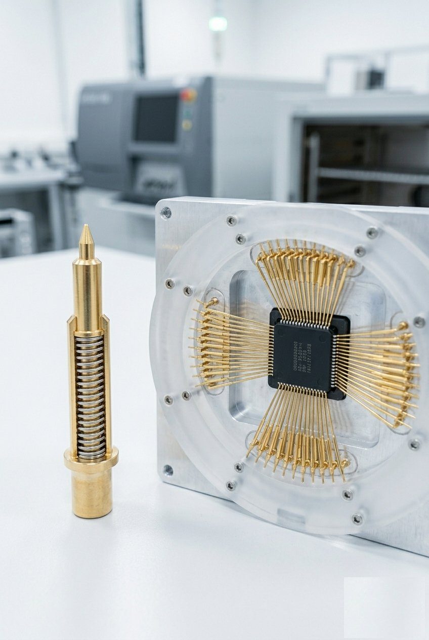
Focusing on C.C.P.’s proprietary products in QFN test modules — from individual DE3-085BB40 test probes to complete application layouts with four-directional array contact to IC pads.
01
02
01
DE3-085BB40 Probe Body
C.C.P. proprietary high-temperature plating Pogo Pin — spring structure housed in barrel, probe tip uses proprietary plating replacing standard 10μ gold plating, maintaining ≤175mΩ contact resistance at 200°C for 500H.
DE3-085BB40-01C0WHigh-Temp PlatingEVT Validated
02
QFN Test Module Probe Array
C.C.P. test probes in four-directional array contact QFN package IC gold-plated pads — providing a stable low-LLCR measurement interface. Proprietary high-temperature plating allows probes to operate long-term without frequent replacement.
QFN Package≤175mΩ500H Stable
Reference Solutions
Recommended Test Probe Solutions
C.C.P.’s flagship semiconductor test probe — proprietary high-temperature plating solves the high-temperature failure problem of standard gold plating.
Total 1 Products
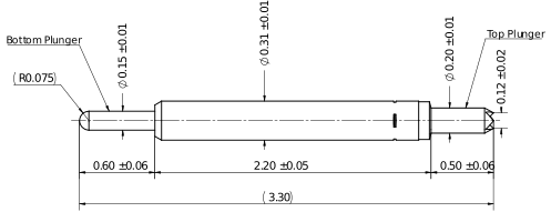
3.30 mm, IC Test Probes, 0.31 mm Diameter, DE3-031DF21-01A0